Compact and Optimized Solar Power Converter
Monday, August 10, 2015
Abstract—This paper will discuss some ground breaking changes in the solar cell converter. There are changes that we have incorporated result in a significant improvement over the present technology. The aim of this paper was to determine a way to reduce the size while improving lifetime of the device, without a compromise to cost.
Keywords—solar; interleaved topology; compact converter; boost converter; ceramic capacitor; syncronous rectification.
I. INTRODUCTION AND BASIC WORKING
Solar is the need of yesterday, which has been delayed by a number of causes. It is one of the technologies that need our immediate and a lot of attention. Since time immemorial solar energy has been reduced to sustain life and agriculture on earth and that has been a gross underutilization of an unlimited, clean source of energy. Our over dependence on fossil fuel, especially post industrial revolution has been a great burden on the environment. The technologies to sustainably harness solar energy have been around for a while now and there has been a lack of focus to commercialize the use of it. Solar energy, when becomes an integral contributor to energy needs of today, we can expect a sea of change towards a better environment. That, notwithstanding, will also reduce the cost of energy production. Fossil fuels are very costly to extract, purify, transport and utilize. This cost will be negated when solar power becomes a major player in the energy scenario. Another advantage, that will come along with the advent of solar energy is, reduction of home electricity consumption charges. There are cases of households which has implemented solar cell panels at their homes and have seen a reduction of up to 80% in their bills. A lot of these homes are in a place where sun is not at its full radiance for a considerable time of year.
Solar panels have a life time of at least 10 years and so does the battery bank. The converter present can operate only for three years. This implies that if we make the converter to be a longer lasting one, the lifespan of entire solar power system goes up to ten years, without major maintenance. The name of our paper, “Four phase interleaved synchronous boost converter” tells everything about the converter we are talking about. “Four phase Interleaved” means we are using multiple phases to divide current so that size of components and load on them are going to be reduced. It will also decreases the numeric
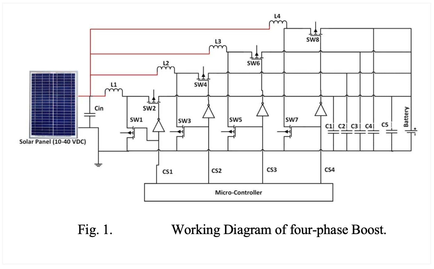
SW1, SW3, SW5 and SW7. The rectification MOSFET are named as SW2, SW4, SW6, and SW8. A micro controller controls these Switching MOSFET. It changes the duty cycle to keep the output voltage constant when there is variable input voltage. The input of this circuit provided by the solar cell which is being exposed to light. The output would be the battery which is being charged. The input voltage from the solar cell varies from ten to forty volts and the output has been fixed to forty eight volts. The input voltage varies due to difference in the intensity of sunlight being emitted over the surface of the solar cell. The converter can be deployed with a variety of solar panels of different output power. Most widely used panels have output wattage of 60, 120, 240 and 300 W.
This brings uniformity and reduced the manufacturing cost of the converter. The capacitors present at the output and at the input are playing an important role of stabilizing current by reducing the ripples.
There are four control signals with a π/4 phase difference, namely, CS1, CS2, CS3 and CS4. The frequency of the input is 150 KHz. That gives our time period to be 6.6 micro seconds between the control signals. When one of the switch (SW) turns on, the inductor present in the immediate circuit starts storing current. That inductor will be charged to it capacity and voltage and the output increases.
II. SIMULATION AND LAYOUT
A. Simulation
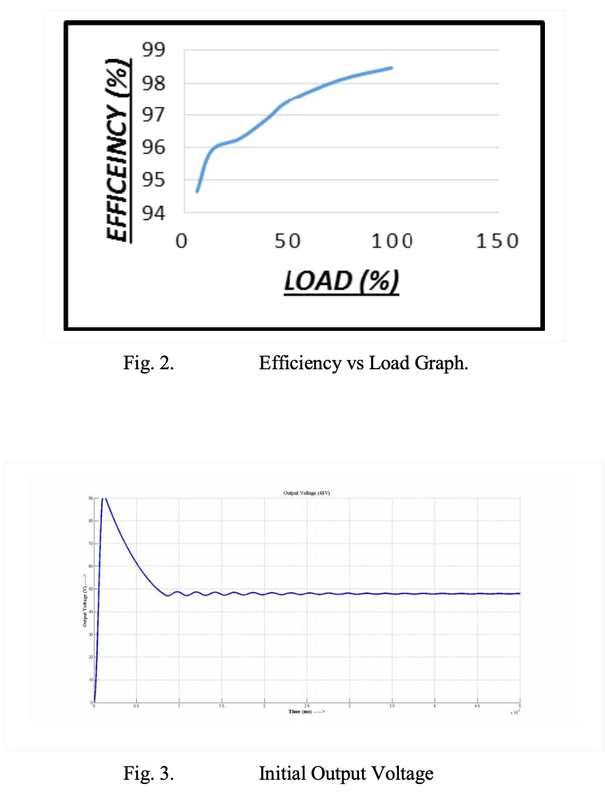
We are using MATLAB-Simulink for simulation. Circuit and working is same as discussed before. We see expected results. Efficiency of converter is increased by 2 percent. Output ripples are also decreased dramatically in comparison to single phase boost converter. Values of capacitors and inductors used in simulation is same as discussed in introduction. We can see the efficiency and percentage load graph in fig. 2 which is really promising. Output voltage is stabilized at 48V after 5ms of turning on the converter as shown in fig. 3.
B. Layout
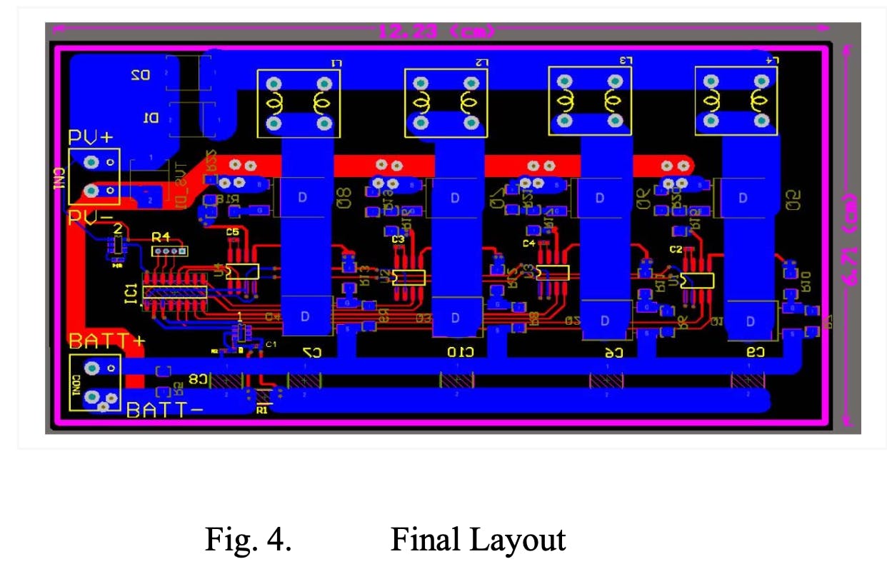
We used Altium to make the schematic and layout of the concept. As result, final printed circuit board size came out to be over 20% more compact than the currently employed converters. For the exact comparison, we took a MPPT converter module of Texas Instruments (PMP 7605) [2]. Its size is 130*84*22 mm. Size of our converter is came out to be 122.3*67.1*20 mm. Fig. 4. Shows the final layout of four phase synchronous converter. The sleek size of this converter allows it to be easily installed behind the junction box.
III. CALCULATIONS
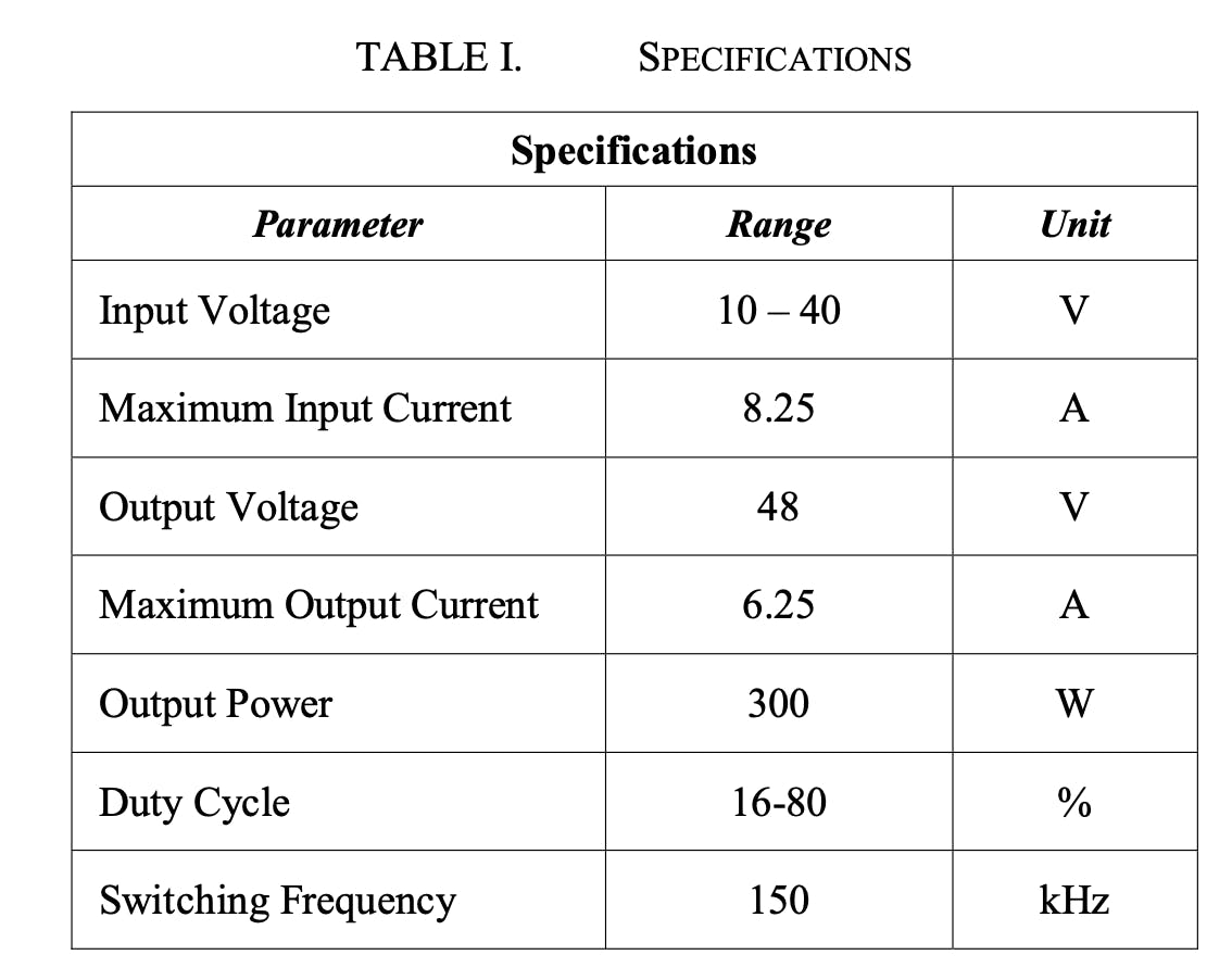
Most challenging and important part of designing of converter is to calculate values of inductor, input and output capacitors. Smooth output, better efficiency and less ripples, are the factors depending on perfect calculated values. For four phase interleaved synchronous boost converter specifications are as in below table I. Calculated values are Inductor of 28 micro Henry and five ceramic output capacitors in parallel, each of 22 micro Farad.
Equations used for calculations are [3]:
A. InductorValue
Here, L = Inductor; Vin (min) = minimum input voltage; Von = On time MOSFET voltage; Dmax = maximum duty cycle; Fs = switching frequency; Iout = Output current.

B. OutputCapacitorValue
Here,
Cout = Output capacitor; Iout = Output current; Dmin = Minimum duty cycle; Fs = switching frequency; ∆Vout = output ripple voltage; Ipeak = peak current; ESR = Equivalent series resistance.

C. Ceramic capacitor availability
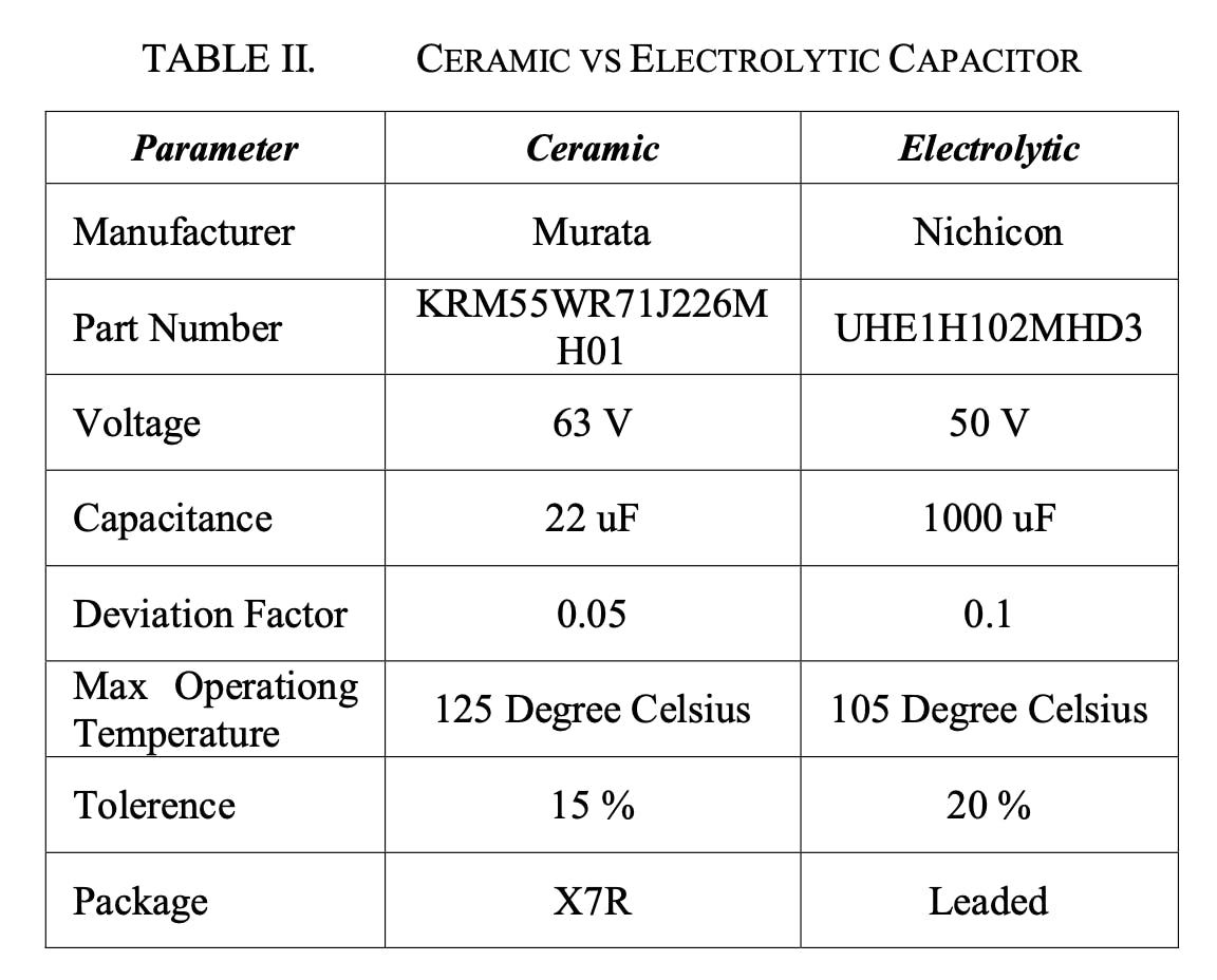
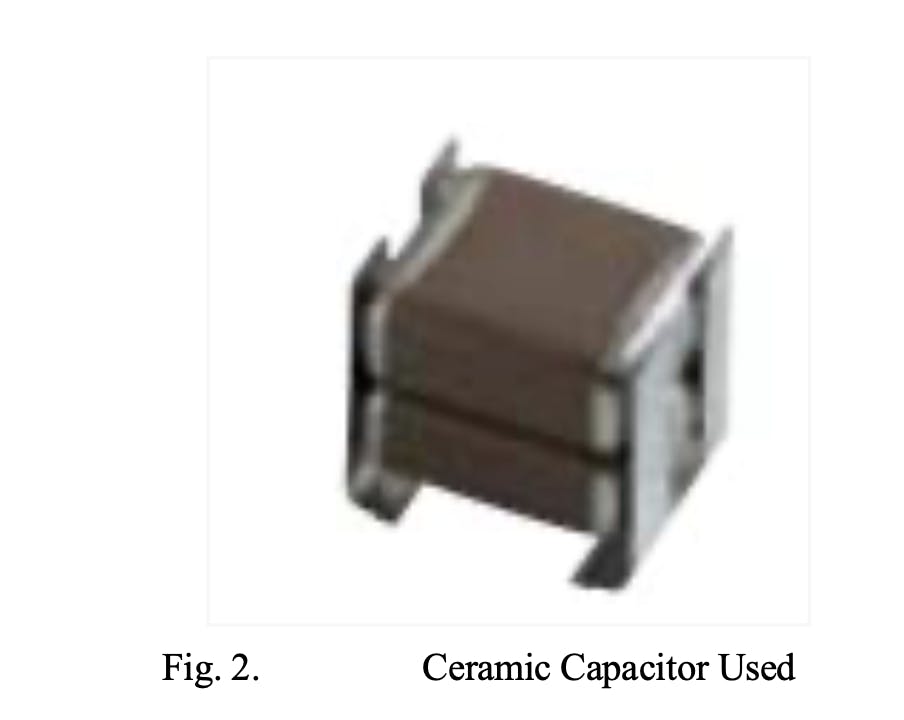
As we calculated, ceramic capacitor of 22uF/ 63V is available to use. The cost of a thousand 22uF ceramic capacitors is $2.04 and cost for thousand 1000uF electrolyte capacitor is $0.72. Whereas, life of the ceramic capacitor is 10 years which is three times that is of electrolyte capacitor. Also, size is decreased by using ceramic capacitor and ripple handling is increased. This also helps in improving the life of converter as capacitor is the component which has lowest life span in converter. The capacitor we have used have a few additional features. One of them is that it has bond metal terminals present at the sides of the chip as seen in Fig 5. This helps to reduce the stress experienced by the capacitor by its elastic effect. Another advantage is that it is easier to fabricate over the permanent circuit board (PCB) and can withstand two thousand cycles of heat stress. The comparison between ceramic and electrolytic capacitor has been tabulated in Table II. [4]
IV. THERMAL MANAGEMENT REQUIREMENT
Ceramic capacitor we chose can withstand sustain considerable amount of heat. This capacitor can function at a temperature of 125 degree Celsius. The thick metal terminals of this capacitor are well suited to conduct and withstand the current flowing. The four phase topology used splits the 8A input current to four parallel branches. This reduces the load on every component and also on PCB tracks. The inductor used for better thermal capabilities, is of higher material, NC95 or equivalent.
The layout has been very carefully thought out for better performance under high heat conditions. The materials used is of grade FR4. The PCB is double sided, 2mm thick and power copper tracks are exposed for better conduction. Wide layer thickness for power tracks are used for better heat distribution. The design allows for lesser strain on each component. The layout is designed in such a way that there is no need for heat sink.
V. COMPARISONS WITH TRADITIONAL TOPOLOGY Below are few advantages over traditional converter:
A. Scalability : The design of our converter enables it to be employed at the backside of each panel. This converter can operates with a large input range and hence, can be utilized with almost any avaiable solar panel. The traditional solar converter has shortcomings on each of the above mentioned frontiers. It is required to be separate from solar panels and are not universally compatible.
B. Cost : The bill of materials for an equivalent converter to our design $24.013. However, the converter we designed has a cost of $32.042. The price of our design is reduced as there is no need of a sperate box for the traditional converter. Wiring costs is also negated for our design.
C. Compactness: Since the dimensions of our converter is came out to be 122.3*67.1*20 mm, the surface area comes to be 23988.66 mm square . The surface area of MPPT converter module of Texas Instruments (PMP 7605) is 130*84*22 mm. The total surface area comes to be 31256mm square. That implies that, our converter is 24% smaller than the traditional converter.
D. Life : The lifespan of electrolytic capacitor 10,000 hours, nearly three and half years. Whilst, ceramic capacitor’s deviation factor is half of that of electrolytic capacitor, which implies that the lifetime is more than thrice of electrolytic capacitor. Hence, converter life is increased by three times.
VI. ISSUES ENCOUNTERED AND SOLUTION
We faced a small number of issues while we were doing our research for this paper. These obstacles, though small in number, were very daunting and required a lot of work to mitigate them. The main obstacle was the stability issue in the face of high frequency control signal. We found that the stability goes down as the frequency increases. We had to make a lot changes in the layout to make sure that stability remains well above industry standards. Another major roadblock we faced was at calculations end. We had to keep in mind the inductor saturation and several other losses that effect our efficiency. It took us a long time and effort to find the capacitor which perfectly fits all our needs. Also, we had to find all the components which would render our converter to be affordable and at a competitive price. We had several talks with a large number of manufacturers to determine which capacitor would be the best for our application.
Also, we were faced with a need of heat sink which would greatly increase the size of our design. That was one of the reasons for us to use four phase, instead of three phase topology. Extra planning and consideration on layout, helped us to design a converter without a heat sink and very little thermal effects.
VII. CONCLUSION
The significant changes in the converter assembly, which arose from our research, have very interesting ramifications.
One of them would be the additional space achieved by the use of ceramic capacitor. This frees up a lot of space to be utilized by either reducing the converter size or including any future advancement. The lifetime of the entire device increases by at least two fold. This means that, the converter will last longer as the capacitor is the component that has the shortest lifespan. This leads to larger scope of improvement in the solar energy development. The size has been reduced to an extent that each panel can now be fitted with a converter on its rear end. We were able to achieve all that we had planned to. This has reduced spaced consumed by the entire solar power system. Now, panels can be more efficiently placed on rooftops with space constraint. This design has the most efficiency of all the converters available today.
ACKNOWLEDGMENT
There are several people who were integral for this paper to be a success. These people were the ones who made significant contribution towards helping us write this paper. We would like to express gratitude to Mr. Sachin Rana and Mr. Abhishek Mathur for being our constant source of support and encouragement. We also would like to include Ms. Geeta Nijhawan and Ms. Vimlesh Singh, whose guidance was precious to our methodology. Our families and friends are also to be thanked for making sure we stay on track and for being with us through thick and thin. Lastly, we would like to thank our respective parents for all that they have done, which has made all this possible. Thank you all once again.
REFERENCES
- [1] Domenico Ragonese, and Massimiliano Ragusa, “Designing with the SVP1020, an interleaved boost converter with MPPT algorithm,” Application Note STmicroelectronics, DOC ID. 018749, rev. 1, May 2012.
- [2] Texas Instruments, “Test report of MPPT charge controller,” Test Report TI, DOC ID. PMP7605, rev. A, April 2013.
- [3] Texas Instruments, “AN – 1962 LM5032 Interleaved boost evaluation board,” User Guide TI, DOC ID. SNVA395A, rev. 2, May 2013.
- [4] Murata, “KRM series specifications,” unpublished.